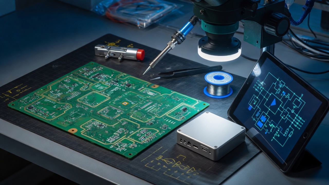
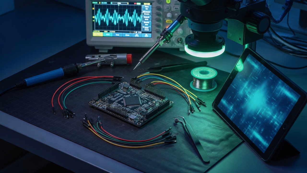
What you leave with
A layout package you can send without a week of cleanup.
- ▸Multilayer digital and mixed-signal
- ▸Power and analog care
- ▸High-speed constraints
- ▸Library and BOM hygiene
Clean copper. Honest constraints. A board your assembler will not send back.
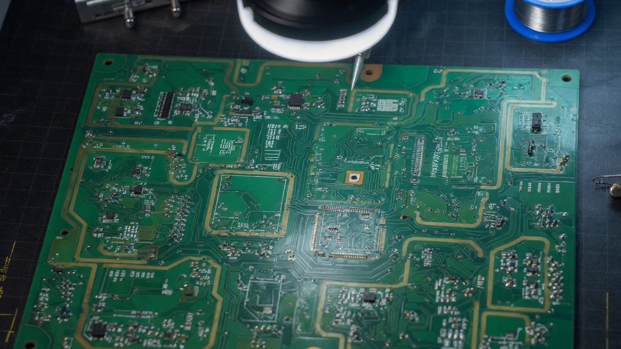
Altium when the team already lives there. KiCad when you want a portable, modern flow. We will not start a religious war; we will match your factory. DRC, BOM, and known risks are called out in plain language.
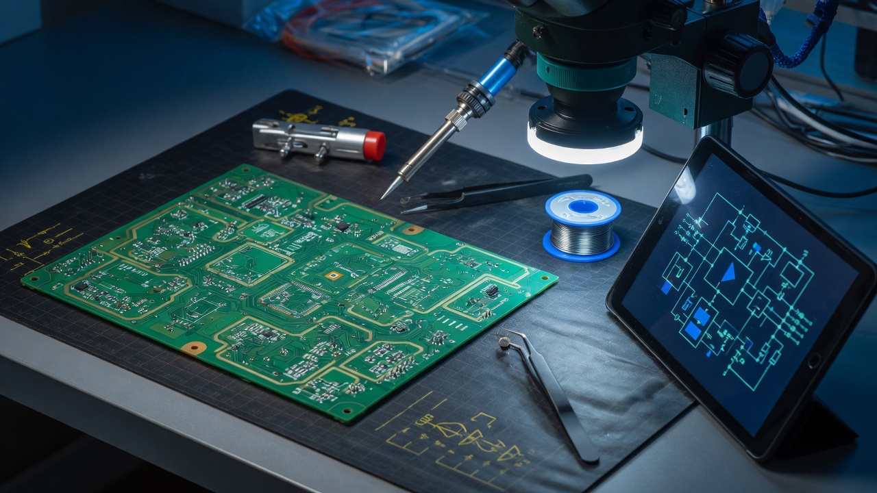
Environment, interfaces, cost, volume, and the parts that are actually in stock.
Capture with the firmware and mechanical people reviewing pinouts early.
Stack-up, placement, and routing that respect signal integrity and thermal reality.
DRC, BOM, gerbers, and the risks written in sentences a CM can read.
A layout package you can send without a week of cleanup.
Product teams who need a senior layout partner for a real spin, not a student board.
Tell us what you are shipping. We will map the work, the team, and a first delivery date.
This site uses cookies to improve your experience and analyze traffic. You can accept all cookies or continue with essential cookies only.
Add PCB Design & Layout to your home screen
Install this site for quick access from your phone or tablet.